Technology Labs
BEL-ADA: Analog to Digital and Digital to Analog Converter Trainer
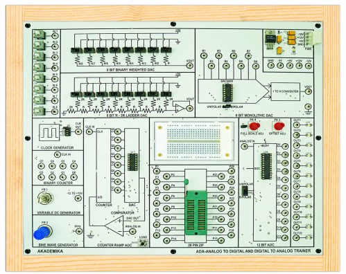
1) Single board system
2) IEEE symbol of all components provided on the PCB.8-bit binary weighted and 8-bit ladder type DAC are constructed using discrete components
3) 8-bit digital ramp ADC constructed using discrete components
4) 12-bit monolithic ADC having conversion time in the range of μs, industry standard pin out, wide input range
5) All Components are visible clearly on the top of the PCB
6) Mobile based Interactive e-Manual
On board components Sine Wave Generator
1) Amplitude : 0V to 5V
2) Frequency : 1KHz
Variable DC Generator
1) Voltage Range : -12V to +12V
Clock Generator
1) Frequency range : 0.5Hz, 1Hz, 2Hz, 4Hz
Digital to Analog Converter
1) 8 bit Binary weighed Resistor DAC
2) 8 bit ladder type D to A converter
3) 8 bit D to A converter using Monolithic IC
Analog to Digital Converter
1) 8 bit discrete ADC
2) 12 bit successive approximation monolithic ADC IC.
Binary counter : 8 bit binary counter with external clock
Output : 12 LED’s to observed ADC output
Interconnection : 2mm connectors
Power Supply : -12V, +12V,+5V,GND
Analog to digital converter
1) To study and measure resolution of ADC
2) To measure the conversion time of the ADC
3) To study full scale adjustment for unipolar and bipolar signals
4) To study the working of ADC
Digital to analog converter1) To study and measure the resolution of DAC
2) To study and measure the settling time of DAC
3) To study the effect of settling time on DAC
4) To study the working of DAC for various digital data pattern
With 35 years of legacy in Technical Education, Akademika extends its expertise to Defence and Skill development, building Innovative, Reliable Training Systems for the next generation of Learners.
Partner with Akademika
Join leading institutions that trust our engineering to Advance Learning and Research.