Technology Labs
PCB-B: Basic PCB Manufacturing Lab
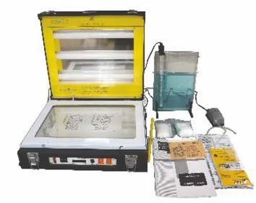
About Product
A complete hands-on PCB prototyping setup for engineering students to design and manufacture single-layer PCBs in-house. It includes UV exposure, etching, drilling, and material preparation accessories, enabling quick turnaround from circuit design to working PCB within hours—ideal for practical electronics education and product development fundamentals.
PCB Lab allows you to produce custom prototype quality circuit boards in a few hours with inexpensive equipment. Short development cycles have previously been restricted to the domain of software projects. Hardware designers can now benefit from improved, if still somewhat slow, cycle times
Akademika‘s Basic PCB Lab covers all the standard processes for manufacturing of PCB. Necessary Item required for each process are provided as a standard set. An exhaustive user manual is provided along with this lab with easy to understand steps to make PCB without any error.
LAMINATES
High sensitive photo resist coated
Short exposing time : 60~90 Second
Color varied after exposure
PCB Thickness: 1.6mm
Copper Thickness : 0.5-24mm
Track Thickness : 0.4mmPCB Type and Size
PS- 10X15CM : 10 each
PCB ARTWORK PAPER
Transparent papers : 20
Size: A4UV EXPOSURE BOX
Supply voltage : 240V, 50Hz
Power(Max) : 200W
UV source : 4x15W Fluorescent Lamp
Mask area : 22x37cm.DEVELOPER
Chemical: DP-50
Weight: 500gmETCHANT
Weight: 500gm
Chemical : ET-20ETCHING TANK
Etching: ET-20
Tank capacity : 2 Liters
Dimension: 360X280X40MMHEATER
EPH-20Temperature adjustment : 35°C to 55°C
Waterproof double insulation
Power lamp indicates ON/OFF cycle
Heating elements with improved insulation
Heater rating : 300W /230V ACAir Pump
Voltage: 230V/50Hz
Power: 3WPCB Drilling Machine
Drilling capacity : 0-3mm
Spindle speeds (in R.P.M)
Speed stage (Stepless): 2000 – 2600.
With 35 years of legacy in Technical Education, Akademika extends its expertise to Defence and Skill development, building Innovative, Reliable Training Systems for the next generation of Learners.
Partner with Akademika
Join leading institutions that trust our engineering to Advance Learning and Research.