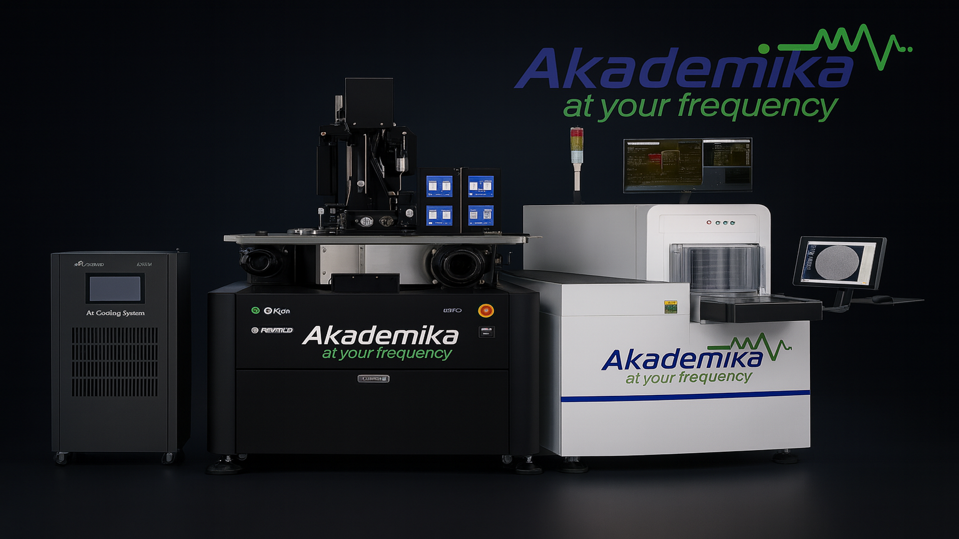

As semiconductor technologies advance toward smaller nodes and higher integration, wafer-level accuracy and repeatability have become critical to device performance and yield. Akademika Probe Stations are engineered to meet these demands by delivering high-precision, automated wafer probing solutions for semiconductor testing, validation, and research.
Designed for reliability and scalability, Akademika Probe Stations enable seamless wafer handling, accurate probe alignment, and consistent electrical contact across repeated test cycles. Whether deployed in R&D environments, academic cleanrooms, or industrial test labs, our systems support efficient characterization of semiconductor devices while minimizing operator dependency and human error.
By integrating robust mechanical design with advanced motion control and test compatibility, Akademika’s probe stations help users achieve higher throughput, lower test variability, and faster time-to-results. These capabilities are essential for applications ranging from device development and process optimization to quality assurance and training.
Aligned with India’s growing semiconductor ecosystem, Akademika is committed to providing industry-grade probe station solutions that strengthen indigenous capabilities in wafer-level testing and semiconductor education. With a focus on precision, durability, and user-centric design, Akademika Probe Stations empower innovators to test with confidence — at every stage of the silicon journey.