
Technology Labs
VL-SPARTAN7 - Spartan-7 SoM with Basic Carrier Board
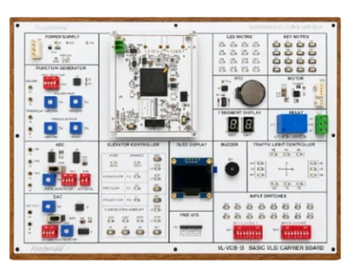
1 ) Based on FPGA Spartan-7 XC7S50-1FGGA484I
2) SOM Interface : high-density board-to-board for SOM
3) 87mm x 67 mm board size Compact form factor
4) Linux BSP, tool chain and Support availableIndustrial Grade, Rugged platform
5) On module required power supplies for efficient power management
6) Linux board support package along with Root file system enables seamless integration
7) Customized Carrier boards for instant board bring-up and quick prototyping
CONFIGURATION & I/O
1) FPGA configuration through USB JTAGOn-board breadboard ·
2) 6 free I/Os on connector
3) JTAG-to-USB programming cable provided
4) Software for Spartan-7 : VIVADO
2) SOM Interface : high-density board-to-board for SOM
3) 87mm x 67 mm board size Compact form factor
4) Linux BSP, tool chain and Support availableIndustrial Grade, Rugged platform
5) On module required power supplies for efficient power management
6) Linux board support package along with Root file system enables seamless integration
7) Customized Carrier boards for instant board bring-up and quick prototyping
CONFIGURATION & I/O
1) FPGA configuration through USB JTAGOn-board breadboard ·
2) 6 free I/Os on connector
3) JTAG-to-USB programming cable provided
4) Software for Spartan-7 : VIVADO
System on Module Board
1) Device: FPGA SPARTAN 7 XC7S50-1FGGA484IDDR3: 256 Mbit,
2) DDR3JTAG: On-board standard JTAG connector, 14-pin, 2 mm pitch, dual row
3) Flash: On-board programming Flash, 128 MB
4) IOs: 3 Nos. of I/O 0.8 mm board-to-board connectors with max. 169, 3.3 V I/Os
OPTIONAL Interface Present on SOM Hardware
1) LEDs: On-board 3 LEDs for indications
2) EEPROM: I2C EEPROM, 1 Mbit size
3) DEBUG: UART debug interface over USB Type-C connector
4) USB: On-board 2 USB 2.0 Type-A connectors, self-powered USB ports
CARRIER BOARD
CARRIER - CORE, RESET & DEBUG
i) Power : Regulated supply as per SOM & peripheral load 1.2V, 2.5V, 3.3V
ii) RTC : External real-time-clock provision
iii) Test points : For important signals and power rails
iv) SOM Interface : high-density board-to-board for SOM
v) On board 50MHz clock and Power On reset circuit.
CARRIER - FUNCTION GENERATOR
i) Square and triangular wave generation
ii) Frequency variable 4 KHz–40 KHz with fine & coarse selection (both waves)
iii) Amplitude variable 0–2 Vp-p for square and triangular wave
iv) Offset adjustment for triangular wave
ANALOG INPUTS
i) Anti-aliasing filter at ADC input (ch 1) with time-constant adjustment
ii) ADC AD7934 (12-bit) with 4 channels
iii) Thermistor interface on ADC channel 4
ANALOG OUTPUT
i) Reconstruction filter at DAC output with time-constant adjustment
ii) DAC TLV5619 (12-bit, 100 ns conversion time)
USER INTERFACE
i) 16 input switches . 4×4 LED matrix
ii) 4×4 matrix keyboard
iii) Two 7-segment displays · OLED display
CONFIGURATION & I/O
i) On-board breadboard · 6 free I/Os on connector
FSM APPLICATIONS (ON-BOARD)
i) Traffic light controller
ii) Elevator controller
MOTOR - RELAY - RTC - BUZZER
i) Stepper motor : 5 VDC, 25–100 steps/sec
ii) DC Motor : 5 V
iii) Relay : One NO & NC contact via 5 VDC relay
iv) RTC : Real-time clock via I²C bus
v) Buzzer : On-board buzzer interface
SOFTWARE
AMD Vivado Design Suite is a software tool used to build and program digital hardware for AMD adaptive SoCs (System on Chips) and FPGAs (Field Programmable Gate Arrays)
Design Entry: Write hardware code using VHDL or Verilog, or use visual block diagrams via the IP Integrator.
Synthesis: Change your high-level code into a gate-level netlist optimized for your specific chip.
Implementation: Handle the physical Place and Route steps to connect logic cells and meet timing limits.
Verification: Simulate and test designs before loading them onto real hardware.Bitstream Generation: Create the final binary file (.bit) needed to program the FPGA.
Hardware-centric design: Used for creating the physical digital logic on the FPGA fabric.
Core tasks: Handles design entry (writing Verilog, VHDL, or block diagrams), synthesis, place-and-route, and timing/power verification.
Output: Generates the hardware bitstream and an XSA (Xilinx Support Artifact) file, which describes the hardware layout for software tools.
1) Device: FPGA SPARTAN 7 XC7S50-1FGGA484IDDR3: 256 Mbit,
2) DDR3JTAG: On-board standard JTAG connector, 14-pin, 2 mm pitch, dual row
3) Flash: On-board programming Flash, 128 MB
4) IOs: 3 Nos. of I/O 0.8 mm board-to-board connectors with max. 169, 3.3 V I/Os
OPTIONAL Interface Present on SOM Hardware
1) LEDs: On-board 3 LEDs for indications
2) EEPROM: I2C EEPROM, 1 Mbit size
3) DEBUG: UART debug interface over USB Type-C connector
4) USB: On-board 2 USB 2.0 Type-A connectors, self-powered USB ports
CARRIER BOARD
CARRIER - CORE, RESET & DEBUG
i) Power : Regulated supply as per SOM & peripheral load 1.2V, 2.5V, 3.3V
ii) RTC : External real-time-clock provision
iii) Test points : For important signals and power rails
iv) SOM Interface : high-density board-to-board for SOM
v) On board 50MHz clock and Power On reset circuit.
CARRIER - FUNCTION GENERATOR
i) Square and triangular wave generation
ii) Frequency variable 4 KHz–40 KHz with fine & coarse selection (both waves)
iii) Amplitude variable 0–2 Vp-p for square and triangular wave
iv) Offset adjustment for triangular wave
ANALOG INPUTS
i) Anti-aliasing filter at ADC input (ch 1) with time-constant adjustment
ii) ADC AD7934 (12-bit) with 4 channels
iii) Thermistor interface on ADC channel 4
ANALOG OUTPUT
i) Reconstruction filter at DAC output with time-constant adjustment
ii) DAC TLV5619 (12-bit, 100 ns conversion time)
USER INTERFACE
i) 16 input switches . 4×4 LED matrix
ii) 4×4 matrix keyboard
iii) Two 7-segment displays · OLED display
CONFIGURATION & I/O
i) On-board breadboard · 6 free I/Os on connector
FSM APPLICATIONS (ON-BOARD)
i) Traffic light controller
ii) Elevator controller
MOTOR - RELAY - RTC - BUZZER
i) Stepper motor : 5 VDC, 25–100 steps/sec
ii) DC Motor : 5 V
iii) Relay : One NO & NC contact via 5 VDC relay
iv) RTC : Real-time clock via I²C bus
v) Buzzer : On-board buzzer interface
SOFTWARE
AMD Vivado Design Suite is a software tool used to build and program digital hardware for AMD adaptive SoCs (System on Chips) and FPGAs (Field Programmable Gate Arrays)
Design Entry: Write hardware code using VHDL or Verilog, or use visual block diagrams via the IP Integrator.
Synthesis: Change your high-level code into a gate-level netlist optimized for your specific chip.
Implementation: Handle the physical Place and Route steps to connect logic cells and meet timing limits.
Verification: Simulate and test designs before loading them onto real hardware.Bitstream Generation: Create the final binary file (.bit) needed to program the FPGA.
Hardware-centric design: Used for creating the physical digital logic on the FPGA fabric.
Core tasks: Handles design entry (writing Verilog, VHDL, or block diagrams), synthesis, place-and-route, and timing/power verification.
Output: Generates the hardware bitstream and an XSA (Xilinx Support Artifact) file, which describes the hardware layout for software tools.
Implementation and verification of Verilog
1) 8:1 MUX.
2) T-flipflop,D-flipflop, RS-flipflop, JK-flipflop
3) BCD counter, Down Counter.
4) 8-bit bidirectional shift register.
5) 4-bit comparator.
6) Active low 2:4 Decoder
7) 8:3 priority encoder.
8) Binary to gray converter.
9) Full Ripple Carry adder and
10) Full Ripple Borrow Subtractor.
11) 4-bit ALU. a. BODMAS Rule.
12)PRBS generator.
13) LED Matrix testing.
14) Keyboard testing.
15) Buzzer, Relay.
16) OLED testing. temperature display on OLED.
17) RTC display on OLED.
18) Traffic Light Controller.
19) Elevator Controller.
20) Many and more Experiment Support.
1) 8:1 MUX.
2) T-flipflop,D-flipflop, RS-flipflop, JK-flipflop
3) BCD counter, Down Counter.
4) 8-bit bidirectional shift register.
5) 4-bit comparator.
6) Active low 2:4 Decoder
7) 8:3 priority encoder.
8) Binary to gray converter.
9) Full Ripple Carry adder and
10) Full Ripple Borrow Subtractor.
11) 4-bit ALU. a. BODMAS Rule.
12)PRBS generator.
13) LED Matrix testing.
14) Keyboard testing.
15) Buzzer, Relay.
16) OLED testing. temperature display on OLED.
17) RTC display on OLED.
18) Traffic Light Controller.
19) Elevator Controller.
20) Many and more Experiment Support.
With 35 years of legacy in Technical Education, Akademika extends its expertise to Defence and Skill development, building Innovative, Reliable Training Systems for the next generation of Learners.
Partner with Akademika
Join leading institutions that trust our engineering to Advance Learning and Research.